| |
Path Leading Invention
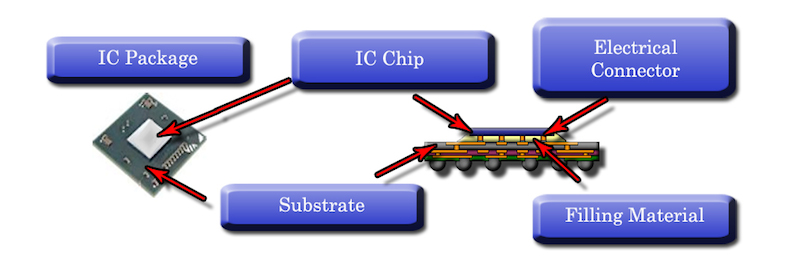
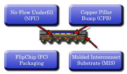
APSI aims to establish its Fine-pitch Flip-Chip Solution that enables high performance, low cost & miniaturized packages utilizing Copper Pillar Bump & Molded Interconnect Substrate to be the de facto standard in semiconductor packaging manufacturing. There are four core areas of innovation in the APSI fine-pitch Flipchip Solution: 1) Copper Pillar Bump (‘CPB’), 2) Molded Interconnect Substrate (‘MIS’), 3) No-flow Underfill (‘NFU’), and 4) Flipchip packaging. Flipchip is a method for interconnecting semiconductor devices to external circuitry with solder bumps that have been deposited onto the chip pads. It has the potential to eliminate wire-bonds which has performance limitations when the line-width becomes smaller and the package density increases.
|
 |