
 |
||
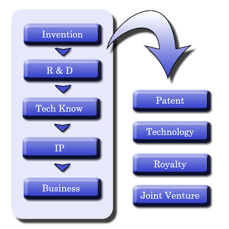
Business Model Back in 2004, APSI developed a light fixed-asset, R&D-focused strategy that leveraged heavily on its industry partners. Consequently, the Company formed its first joint venture with Jiangsu Changjiang Electronics Technology Co Ltd to start Jiangyin Changdian Advanced Packaging Co Ltd (“JCAP”) for high volume manufacturing of semiconductor devices in China using flip-chip process. Subsequently, APSI formed another joint venture called Unisem Advanced Technology Sdn Bhd (“UAT”) with Unisem Bhd in Malaysia. To date, both the CPB technology and MIS technology has been licensed to more than 15 licensees in total to Integrated Device Manufacturers, bumping entities and Outsourced Assembly and Test companies. By selling licenses to downstream semiconductor manufacturers, the Company can proliferates its technologies in the industry much faster than it could do on its own as it leverages on its network of leading semiconductor customers to spread the technologies across broadly. This business model greatly reduces the capital investment and operational costs of APSI that would have been needed were it to manufacture the products by itself. By opting to license its technologies to potential customers, the Company can focus on its research and development, which is its core competence. A further benefit of this model is that by working closely with leading edge downstream manufacturers, the Company can more deeply appreciate the manufacturing challenges faced by these manufacturers. Under the culture of innovation in APSI, such insights often spur innovations to improve the Company’s existing technologies or even lead to ideas for new, as-yet, undeveloped technological solutions for the IC packaging industry. Increasingly, research and development in the Company occurs within an eco-system of equipment and material suppliers, potential customers, research institutions and service providers. Such an open innovation model cuts down on development cost and time and reduces the time for adoption of new technology by customers. The Company has also taken on the approach of promoting its technologies directly to end-user manufacturers, which has the effect of creating a network effect of derived demand for its technologies. As these end users understand the advantages of APSI’s advanced packaging structures and materials, its CPB and MIS, they would ask for new package designs that incorporate such technologies from their suppliers who in turn have to approach the Company for license rights. |
 |
|
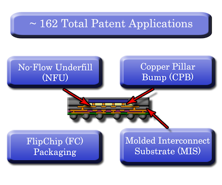
IP Management APS’s major technology breakthrough and innovations are carefully protected by its patent. These patents enabled APSI to successfully transform from a packaging service company into a technology-intensive company. In addition, APSI stands as one of the first IP owners of the Copper Pillar Bump and Molded Interconnect Substrate technology with the earliest priority number related to the innovations. |
||
 |
||