| |
A substrate interposes between an IC chip and a motherboard to enable the IC chip to communicate with the motherboard effectively. Typically, the IC chip is attached onto the substrate and assembled into an IC package before connecting to the motherboard. It is an essential part of the IC package and is responsible for a successful packaging process. Also, it plays an important role in making the IC chip to become a real product and a real solution for end customers. In the past years, semiconductor technologies were highly driven by PC applications which follow Moore’s law in technology migration. In recent years, the emergence of mobile applications increasingly, become the main driver in the semiconductor industry. These mobile applications requires a new kind of substrate that have ability for making IC packages with smaller form factor, thin profile, better thermal, mechanical and electrical performance.
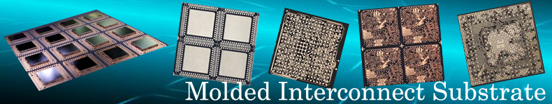
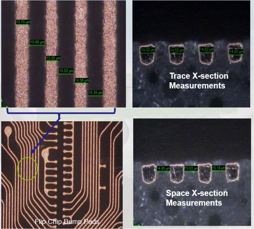
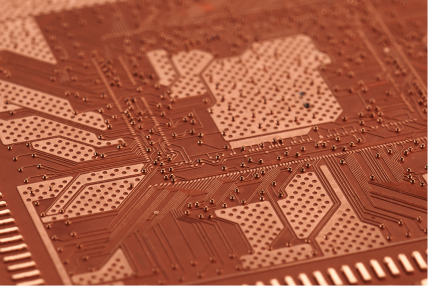
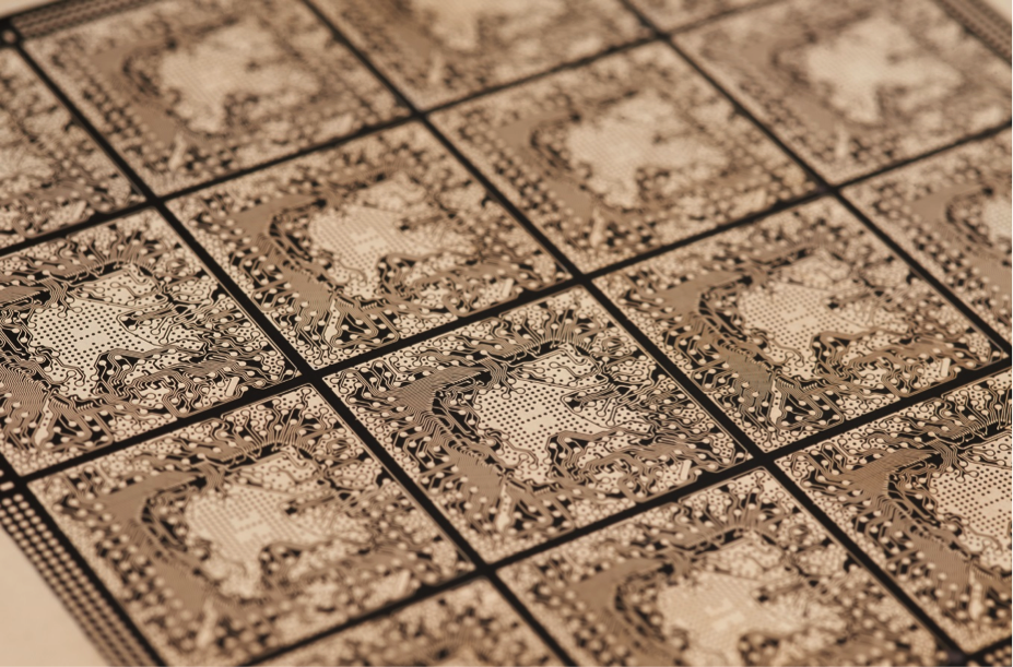
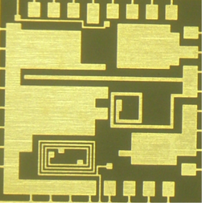
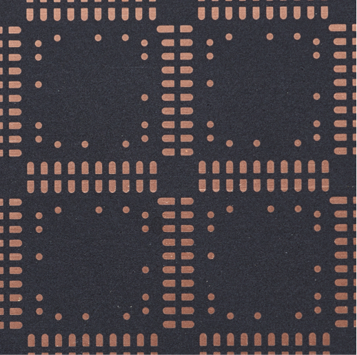
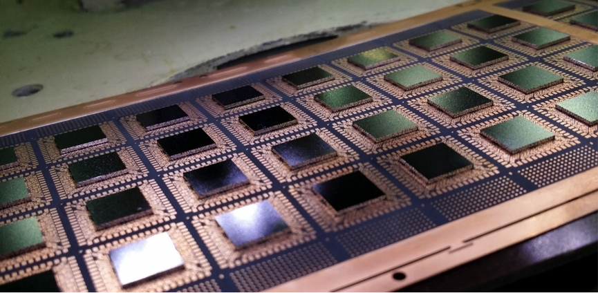
Molded Interconnect Substrate Technology (MIS) is a novel substrate solution that is ideal for mobile industry. It encompasses a wide range of solutions for the complex needs of IC package for mobile applications. With its embedded copper trace technology, it enable a finer line and space that is needed for high I/O count with smaller form factor. It also provides a robust Flip Chip assembly process. Another important feature of MIS substrate is copper filled-via and filled-pad technologies, which is significantly important for high frequency requirements, and improve thermal dissipation.
With the use of the molding materials that have more compatible properties to silicon, MIS substrate improves IC package reliability. The thermal conductivity is also significantly better as heat is dissipated faster within the MIS to prevent overheating of IC chip. Unlike, the materials used for conventional substrate, including BT resin, FR-4, ceramic and polyimide, have thermo-mechanical properties that differ significantly from IC chips that are made of silicon, giving rise to reliability issues due to mismatch in properties.
|