| |
Like in conventional fabrication, integrated circuits are created on the wafer but near the end of the manufacturing process, the attachment pads are metalized on the surface of the chips to make them more receptive to solder. Then solder dots are deposited on each of the pads, and chips are cut, flipped, and positioned so that the solder balls are facing the connectors on the external circuitry. Finally, solder balls are remelted (typically using hot air reflow) and an electrically-insulating adhesive is “underfilled” to provide a stronger mechanical connection, provide a heat bridge, and to ensure the solder joints are not stressed due to differential heating of the chip and the rest of the system.
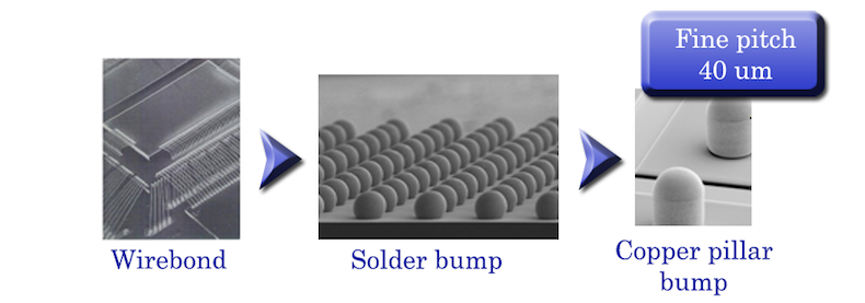
However, as the number of solder balls on a single chip keeps increasing while the size of the chip keeps decreasing, the size of the solder ball also has to decrease. Due to the special shape of the solder ball, |
|
the solder bump solution faces several limitations such as bump pitch limitation, very low standoff, underfill limitation, etc.
APSI invented the copper pillar bump, shrinking the bump pitch by up to 300%, to replace the spherical solder bump as a significant resolution in flip-chip technology. Pillar bump is a novel interconnecting structure, including non-reflowable base and a reflowable cap like a pillar shape. Copper pillar bumps allow finer pitch (<60um) and precise gap control while maintaining sufficient height for mechanical strength. The elongated bumps have thermal and electrical advantages. Such bumps make underfills easier and offer protection from α particles. Moreover, the CPB solution no longer needs a pre-soldered mask substrate and even makes a lead-free option possible. |